- 您现在的位置:买卖IC网 > Sheet目录1234 > NCP1653EVB (ON Semiconductor)BOARD EVAL FOR NCP1653
�� �
�
�NCP1653,� NCP1653A�
�2� Vac� *� 4� V� Vac�
�Ivac� +�
�[�
�IS� +�
�IL�
�Pin� +� ac� +�
�Vout�
�Vcontrol�
�96%� I� ref� ref� I� FB�
�R1�
�Pout� +� h� Pin� +� h�
�Vout�
�stands� for� the� RMS.� I� vac� is� a� constant� in� the� 50� or� 60� Hz�
�bandwidth.� Multiplier� resistor� R� M� is� the� external� resistor�
�connected� to� the� multiplier� voltage� V� M� pin� (Pin� 5).� It� is� also�
�constant.� R� M� directly� limits� the� maximum� input� power�
�capability� and� hence� its� value� affects� the� NCP1653� to�
�operate� in� either� “follower� boost� mode”� or� “� constant�
�output� voltage� mode”.�
�(eq.9)�
�Rvac� )� 12� k� W� R� vac�
�Sense� current� I� S� is� proportional� to� the� inductor� current� I� L�
�as� described� in� (eq.10).� I� L� consists� of� the� high� ?� frequency�
�component� (which� depends� on� di/dt� or� inductor� L)� and�
�low� ?� frequency� component� (which� is� I� L� ?� 50� ).�
�RCS� (eq.10)�
�RS�
�Control� current� I� control� is� a� roughly� constant� current� that�
�comes� from� the� PFC� output� voltage� V� out� that� is� a� slowly�
�varying� signal.� The� bandwidth� of� I� control� can� be�
�additionally� limited� by� inserting� an� external� capacitor�
�C� control� to� the� control� voltage� V� control� pin� (Pin� 2)� in�
�Figure� 30.� It� is� recommended� to� limit� f� control� ,� that� is� the�
�bandwidth� of� V� control� (or� I� control� ),� below� 20� Hz� typically� to�
�achieve� power� factor� correction� purpose.� Typical� value� of�
�C� control� is� between� 0.1� m� F� and� 0.33� m� F.�
�V� reg�
�300� k�
�I� control� =�
�I�
�Regulation� Block�
�over� the� bandwidth� of� 50� or� 60� Hz� and� power� factor� is�
�corrected.�
�Practically,� the� differential� ?� mode� inductance� in� the�
�front� ?� ended� EMI� filter� improves� the� filtering� performance�
�of� capacitor� C� filter� .� Therefore,� the� multiplier� capacitor� C� M�
�is� generally� with� a� larger� value� comparing� to� the� filter�
�capacitor� C� filter� .�
�Input� and� output� power� (P� in� and� P� out� )� are� derived� in�
�(eq.13)� when� the� circuit� efficiency� η� is� obtained� or�
�assumed.� The� variable� V� ac� stands� for� the� RMS� input�
�voltage.�
�V 2 2 RS R vac Icontrol Vref Vac�
�Zin� RM� RCS� Vout�
�(eq.13a)�
�Icontrol Vac�
�T�
�2 RS R vac Icontrol Vref Vac�
�RM� RCS� Vout�
�(eq.13b)�
�Icontrol Vac�
�T�
�Follower� Boost�
�The� NCP1653� operates� in� follower� boost� mode� when�
�I� control� is� constant.� If� I� control� is� constant� based� on� (eq.13),� for�
�a� constant� load� or� power� demand� the� output� voltage� V� out� of�
�the� converter� is� proportional� to� the� RMS� input� voltage� V� ac� .� It�
�means� the� output� voltage� V� out� becomes� lower� when� the� RMS�
�input� voltage� V� ac� becomes� lower.� On� the� other� hand,� the�
�output� voltage� V� out� becomes� lower� when� the� load� or� power�
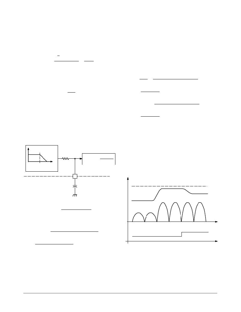
�demand� becomes� higher.� It� is� illustrated� in� Figure� 31.�
�Vcontrol�
�2�
�Ccontrol�
�V� out� (Traditional� boost)�
�Figure� 30.� V� control� Low� ?� Pass� Filtering�
�V� out� (Follower� boost)�
�Ccontrol� u�
�1�
�2� p� 300� k� W� fcontrol�
�(eq.11)�
�V� in�
�From� (eq.7)� ?� (eq.10),� the� input� impedance� Z� in� is�
�re� ?� formulated� in� (eq.12).�
�time�
�Zin� +�
�RM� RCS� Vac� Vout� IL�
�2� RS� R� vac� Icontrol� Vref� IL� ?� 50�
�P� out�
�Zin� +�
�RM� RCS� Vac� Vout�
�2� RS� R� vac� Icontrol� Vref�
�whenIL� +� IL� ?� 50�
�(eq.12)�
�Figure� 31.� Follower� Boost� Characteristics�
�time�
�The� multiplier� capacitor� C� M� is� the� one� to� filter� the�
�high� ?� frequency� component� of� the� multiplier� voltage� V� M� .�
�The� high� ?� frequency� component� is� basically� coming� from�
�the� inductor� current� I� L� .� On� the� other� hand,� the� filter�
�capacitor� C� filter� similarly� removes� the� high� ?� frequency�
�component� of� inductor� current� I� L� .� If� the� capacitors� C� M� and�
�C� filter� match� with� each� other� in� terms� of� filtering� capability,�
�I� L� becomes� I� L� ?� 50� .� Input� impedance� Z� in� is� roughly� constant�
�Follower� Boost� Benefits�
�The� follower� boost� circuit� offers� an� opportunity� to� reduce�
�the� output� voltage� V� out� whenever� the� RMS� input� voltage�
�V� ac� is� lower� or� the� power� demand� P� out� is� higher.� Because�
�of� the� step� ?� up� characteristics� of� boost� converter,� the� output�
�voltage� V� out� will� always� be� higher� than� the� input� voltage�
�V� in� even� though� V� out� is� reduced� in� follower� boost� operation.�
�http://onsemi.com�
�11�
�发布紧急采购,3分钟左右您将得到回复。
相关PDF资料
NCP2993FCT2GEVB
BOARD EVAL NCP2993 AUDIO PWR AMP
NCP345SNT1G
IC DETECTOR OVER VOLTAGE 5TSOP
NCP346SN2T1G
IC DETECTOR OVER VOLTAGE 5TSOP
NCP347MTAITBG
IC OVERVOLTAGE PROT CTRLR 10WDFN
NCP348AEMUTBG
IC MOSFET DRIVER DUAL 12V 10LLGA
NCP360MUTXG
IC CTLR USB POS OVP FET 6-UDFN
NCP361MUTBG
IC USB OVERVOLT PROT CTRLR 6UDFN
NCP3712ASNT3
IC SWITCH OVP HIGH SIDE SC74-6
相关代理商/技术参数
NCP1653GEVB
制造商:ON Semiconductor 功能描述:NCP1653 PFC CCM STEP-UP - Bulk 制造商:ON Semiconductor 功能描述:BOARD EVAL FOR NCP1653
NCP1653P
功能描述:功率因数校正 IC Fixed Frequency RoHS:否 制造商:Fairchild Semiconductor 开关频率:300 KHz 最大功率耗散: 最大工作温度:+ 125 C 安装风格:SMD/SMT 封装 / 箱体:SOIC-8 封装:Reel
NCP1653PG
功能描述:功率因数校正 IC Fixed Frequency Current Mode PFC RoHS:否 制造商:Fairchild Semiconductor 开关频率:300 KHz 最大功率耗散: 最大工作温度:+ 125 C 安装风格:SMD/SMT 封装 / 箱体:SOIC-8 封装:Reel
NCP1654BD133R2G
功能描述:功率因数校正 IC NCP1654 - 133KHZ RoHS:否 制造商:Fairchild Semiconductor 开关频率:300 KHz 最大功率耗散: 最大工作温度:+ 125 C 安装风格:SMD/SMT 封装 / 箱体:SOIC-8 封装:Reel
NCP1654BD200R2G
功能描述:功率因数校正 IC NCP1654 - 200KHZ RoHS:否 制造商:Fairchild Semiconductor 开关频率:300 KHz 最大功率耗散: 最大工作温度:+ 125 C 安装风格:SMD/SMT 封装 / 箱体:SOIC-8 封装:Reel
NCP1654BD65R2G
功能描述:功率因数校正 IC NCP1654-65K-B-SOIC RoHS:否 制造商:Fairchild Semiconductor 开关频率:300 KHz 最大功率耗散: 最大工作温度:+ 125 C 安装风格:SMD/SMT 封装 / 箱体:SOIC-8 封装:Reel
NCP1654BP65G
功能描述:功率因数校正 IC NCP1654-65K-B-PDIP RoHS:否 制造商:Fairchild Semiconductor 开关频率:300 KHz 最大功率耗散: 最大工作温度:+ 125 C 安装风格:SMD/SMT 封装 / 箱体:SOIC-8 封装:Reel
NCP1654PFCGEVB
功能描述:电源管理IC开发工具 NCP1654 PWR FACT CONT EVB
RoHS:否 制造商:Maxim Integrated 产品:Evaluation Kits 类型:Battery Management 工具用于评估:MAX17710GB 输入电压: 输出电压:1.8 V